MRes 2000M Manual Contactless Resistivity Measurement System
Tailored for scenarios where automatic mapping is not necessary
EXCELLENCE
The Cogent Manual System
MRes 2000M Manual Contactless Resistivity Measurement System
[300 mm]
Introducing the MRes 2000M Manual, a manual iteration of our renowned non-contact resistivity measurement system tailored for scenarios where automatic mapping is not necessary.
The MRes2000M empowers users to position samples with precision within the sensor region using a linear transfer line, while upholding the unmatched accuracy and reliability synonymous with the MRes2000 series.
The versatile solution
Designed to accommodate wafer diameters ranging from 100 mm to 300 mm and thicknesses spanning 150 µm up to 1,200 µm, the MRes 2000M stands as a versatile solution. Its adaptability makes it indispensable for a diverse range of applications, particularly in research and development across industries and academia.
Measuring Data
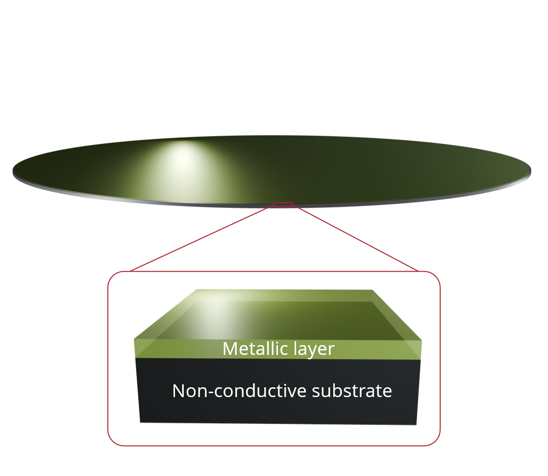
The manually controlled MRes2000M features a standard resistance range of 0.005 Ω/sq up to 100 kΩ/sq, ensuring precise measurements for bulk samples and conductive layers on one side of the wafer.
No Recalibration Needed for any Thickness
Its standout feature lies in its ability to maintain accuracy without requiring recalibration across the entire dynamic range, encompassing both thickness and resistivity variations. With a standard deviation (1𝜎) of less than one percent, consistency is guaranteed in every measurement.
Tailoring measurement results to perfection is made possible through custom-made recipes, covering a spectrum of basic sample properties such as substrate properties and potential film resistivity, especially crucial for semiconductor applications The MRes2000 offers unparalleled flexibility, allowing precise measurement of resistance, resistivity, and thickness across the complete dynamic range without the need for time consuming recalibration.
Seeking an automatic wafer positioning system? Explore our range of other products For any questions or specific requirements, feel free to reach out.
At SWS-Tec, we are committed to advancing your measurement needs with cutting-edge technology.
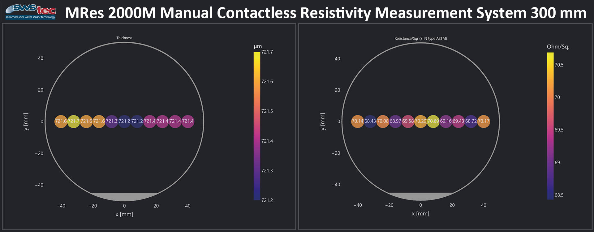
MRes2000M Manually Measured Mapping Result: The MRes2000M system provides manually measured mapping results, exemplified here for a Ø 100 mm Silicon wafer. Eleven distinct measurement points across the wafer are selected for measuring both thickness and resistance, allowing for the quantification of wafer quality.
We are here to help!
Information you provide in the form is used and stored to process your enquiry and, if you have allowed the cookies, to improve content personalisation.
SWS-Tec processes personal information responsibly. For more information, please review our Privacy Policy (General Data Protection Regulation/GDPR).
* Mandatory field
Office
D-85643 Steinhoering, Germany
Hours
M-F: 9am – 5pm
S-S: Closed
Call Us
Why Do We Need Non-Contact Eddy-Current-Based Resistance Measurement?
Traditional resistance measurement methods may involve direct contact, which can alter the properties of the material or even damage delicate samples. Non-contact methods, particularly those based on eddy currents, offer a solution by allowing measurements without physical contact, preserving the integrity of the sample. Eddy current based resistance measurement relies on the principles of electromagnetic induction and the interaction of eddy currents with the material under test.
Principle of Eddy-Currents
Electromagnetic Induction:
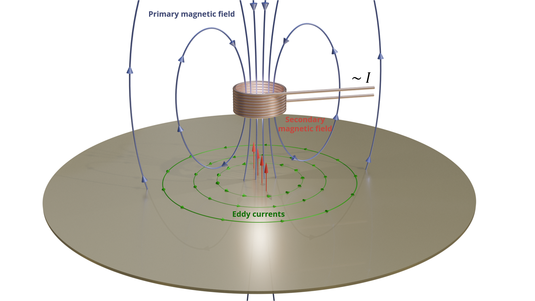
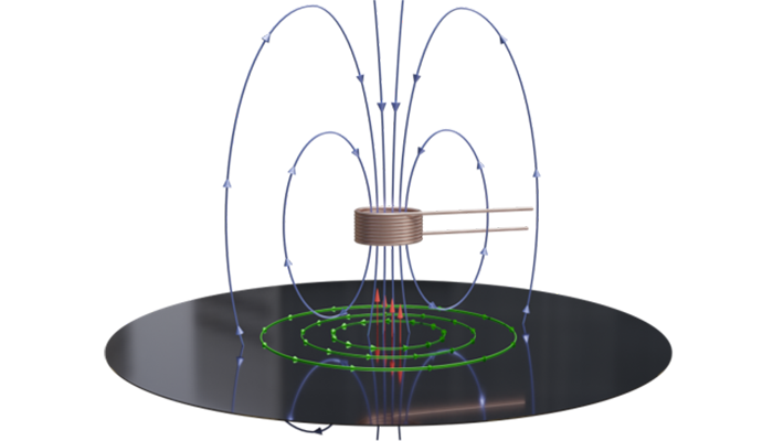
When an alternating current (~ 𝐼) flows through a coil, it generates a time-varying magnetic field around it (primary magnetic field). According to Faraday’s Law of Induction, a changing magnetic field induces an electric current (eddy currents) in a nearby conductive material.
Opposition to Primary Magnetic Field:
The eddy currents create their own magnetic field (secondary magnetic field), which opposes the original magnetic field from the coil (Lenz’s Law). This opposition affects the impedance (Z) of the coil.
For a more detailed explanation of why and how eddy currents can be used to measure the resistance of a material please check out our technology page.
Eddy-Current Based Layer Thickness Measurement for Precision and Reliability
Our advanced layer thickness measurement technology utilizes an eddy-current-based, non-contact approach to provide highly accurate, non-destructive measurements. Designed for delicate and conductive layers, our layer thickness measurement system ensures precise readings without compromising material integrity. This innovative eddy-current-based layer thickness measurement solution is ideal for applications requiring fast, reliable results in quality control and manufacturing. Experience the advantages of non-contact layer thickness measurement for enhanced precision and efficiency across a variety of materials and layers.
Key Applications:
- Thin-Film Technologies: Ideal for assessing thin-film materials after deposition processes like PVD, CVD, MBE and ALD.
- Semiconductor Applications: Suitable for a wide range of semiconductor materials, like Si, GaN and SiC, supporting both research and production needs.
- Solar and Photovoltaic Applications: Designed to measure and optimize materials used in solar cells and other photovoltaic technologies.
- Innovative Glass Technologies: Applicable to architectural glass such as Low-E (low emissivity) glass and smart glass technologies.
- Lighting and Display Technologies: Supports OLED and LED material testing and development.
A Superior Alternative to the 4-Point Probe Technique
Non-Contact, Non-Destructive Eddy-Current Based Measurement
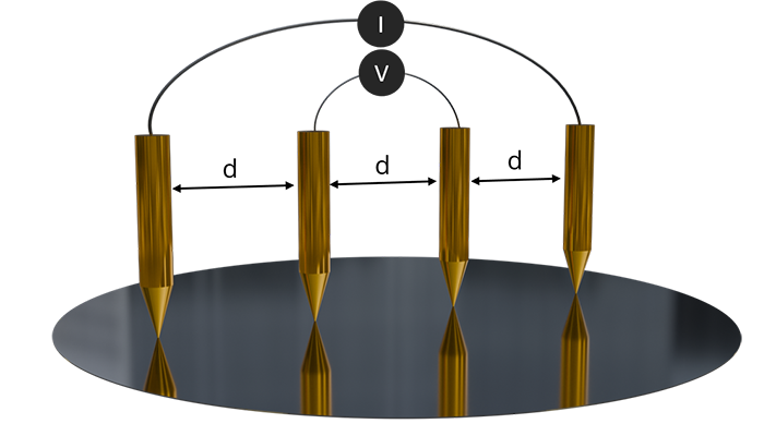
Our eddy-current-based measurement technology offers a powerful, non-contact, and non-destructive solution for both layer thickness and sheet resistance measurements. Unlike the traditional 4-point probe technique, which requires physical contact and may risk damage to delicate surfaces, our non-contact eddy-current approach preserves material integrity by eliminating any physical contact during the measurement process. This non-destructive method not only ensures the longevity of sensitive materials but also provides faster, repeatable results across various applications.
Non-Contact Non-Destructive
For both layer thickness measurement and sheet resistance or resistivity analysis, the eddy-current based technique delivers unmatched precision, efficiency, and durability compared to the 4-point probe. By avoiding surface damage and offering consistent, high-accuracy results, our non-contact, non-destructive measurement technology is the ideal choice for quality control and production environments where both accuracy and material preservation are paramount.
SWS-Tec’s Advanced Eddy-Current Technology for Sheet Resistance Measurement
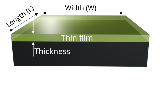
Sheet Resistance Thin Film – Our eddy-current-based sheet resistance measurement technology provides a highly accurate, non-contact sheet resistance solution. Unlike traditional methods, our non-contact sheet resistance approach ensures precise measurements without damaging materials. Designed for advanced applications, our eddy current-based sheet resistance measurement system can reliably measure sheet resistance across a range of conductive materials, delivering consistent, non-destructive results. Whether you’re looking to enhance quality control or boost production efficiency, our sheet resistance technology meets the highest standards for accuracy and reliability.
For a more detailed explanation about sheet resistance please check out our technology page.
Precision Sheet Resistance Measurement on Thin Films
Sheet Resistance Thin Film – Our advanced sheet resistance measurement technology is specially optimized for thin films, offering accurate, non-contact measurements that preserve the integrity of delicate layers. Utilizing an eddy-current-based approach, our system provides fast, reliable sheet resistance measurement on thin films without the need for physical contact, making it a non-destructive solution ideal for sensitive materials.
Whether used for quality control in semiconductor manufacturing or material analysis in research, our thin-film sheet resistance measurement system ensures precise, repeatable results across a range of conductive and semi-conductive materials. Experience the efficiency and accuracy of our technology for high-performance thin-film applications, where precision and material preservation are essential.
![SWS-Tec – MRes 2000M [300 mm] MRes 2000M Manual Contactless Resistivity Measurement System 300 mm](https://sws-tec.com/wp-content/uploads/2024/05/MRes-2000M-300mm-Manual-bw.jpg)
