Technology Main
SWS-tec
Technology Main
Non-Contact Measurement Solutions: Preserving Material Integrity
Traditional resistance measurement techniques often involve direct contact with the sample, which can potentially alter its properties or even damage delicate materials. For all wafers and thin films, maintaining structural integrity during measurements is crucial.
Non-contact methods, particularly those utilizing eddy currents, offer a powerful alternative by enabling accurate measurements without physical contact. This preserves the integrity of the sample while enhancing precision and repeatability in data collection.
The Principle of Eddy-Current-Based Measurement
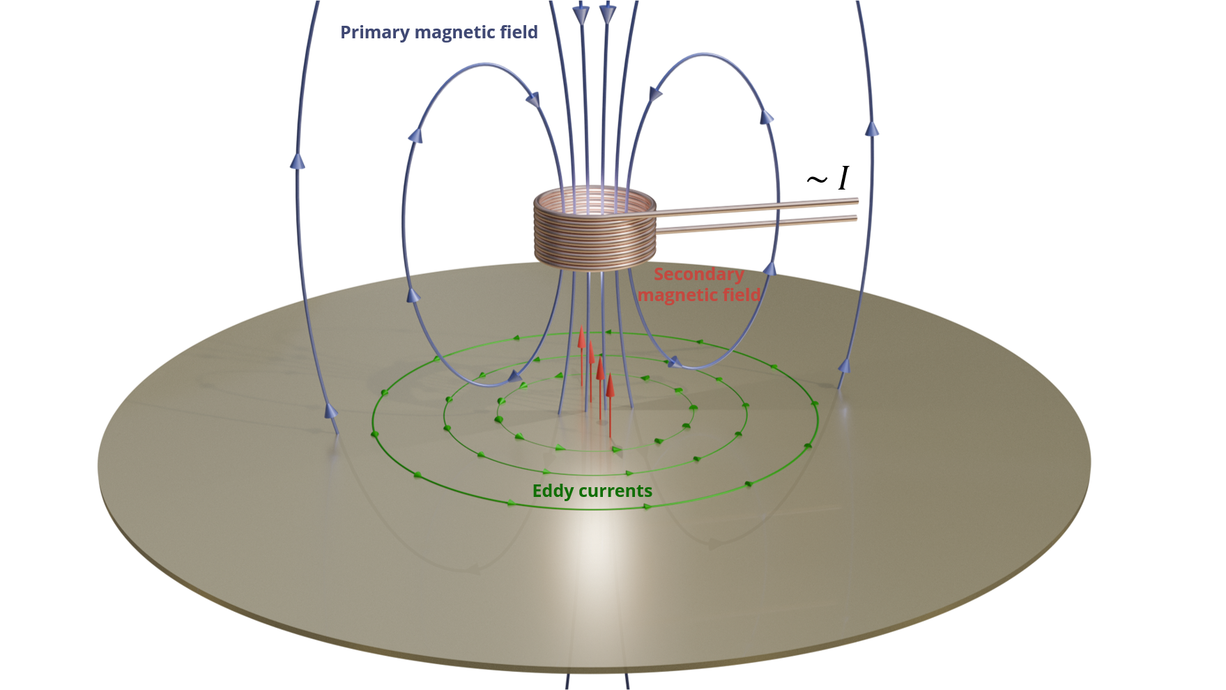
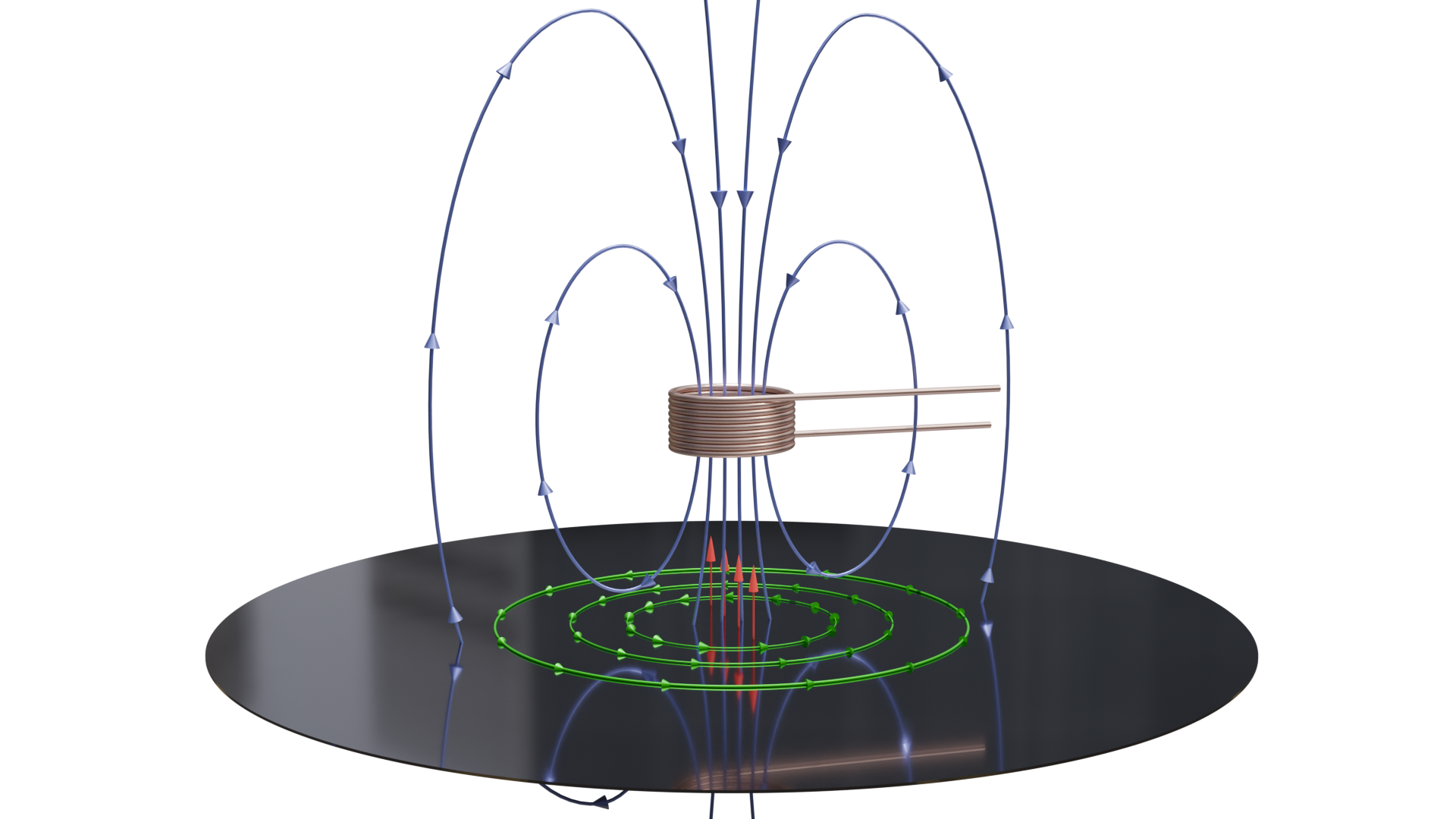
Eddy-current measurement technology operates on the basis of electromagnetic induction. When an alternating current flows through a coil near a conductive surface, it generates an alternating magnetic field.
This field induces circulating currents, known as eddy currents, within the conductive layer. The induced currents generate their own magnetic fields that oppose the original field, causing changes in the coil’s impedance.
By measuring these changes, the system can accurately determine properties such as the sheet resistance and layer thickness of the material.
Advantages Over Traditional Methods
Our eddy-current measurement systems offer a non-contact and non-destructive solution for analyzing both layer thickness and sheet resistance.
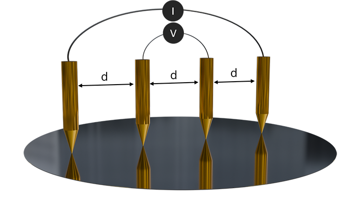
Unlike traditional 4-point probe techniques, which require physical contact with the sample, our system eliminates the need for direct surface interaction. This not only prevents potential surface damage but also improves the longevity of sensitive materials.
The non-contact approach ensures faster measurements with high repeatability, making it ideal for quality control and production environments.
The technique’s precision and efficiency make it particularly valuable for industries such as semiconductors, coatings, and thin films. By eliminating physical contact, eddy-current-based measurements are less prone to wear-and-tear issues, thereby offering superior durability and long-term accuracy.
High-Precision Sheet Resistance Measurement
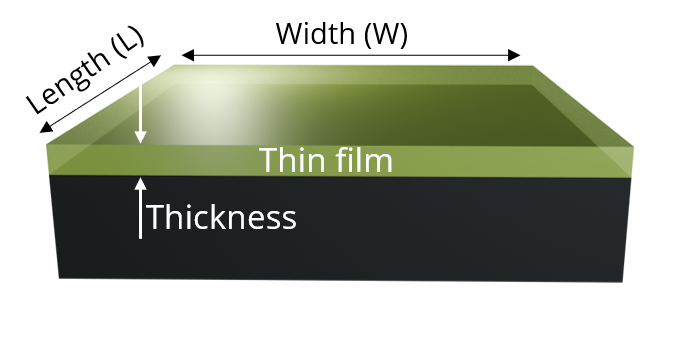
Our advanced sheet resistance measurement technology is optimized for thin films, offering accurate, non-contact measurements that preserve the integrity of delicate layers. This approach uses eddy currents to determine the resistance per unit square of a thin conductive layer.
Since sheet resistance is inherently related to the resistivity and thickness of the material, knowing the resistivity allows for precise calculations of the layer’s thickness.
This precise measurement is achieved without compromising the sample’s physical structure, making it ideal for delicate conductive layers.
Non-Contact Layer Thickness Measurement
In addition to sheet resistance, our layer thickness measurement system employs eddy-current technology to provide accurate, non-destructive assessments of thin conductive layers. Designed to protect delicate and sensitive materials, this system ensures precise measurements while avoiding physical contact.
The ability to achieve fast, reliable readings makes it highly effective for quality control processes, enhancing the precision and efficiency of manufacturing operations.
Capacitive Thickness Measurement for Conductive Wafers
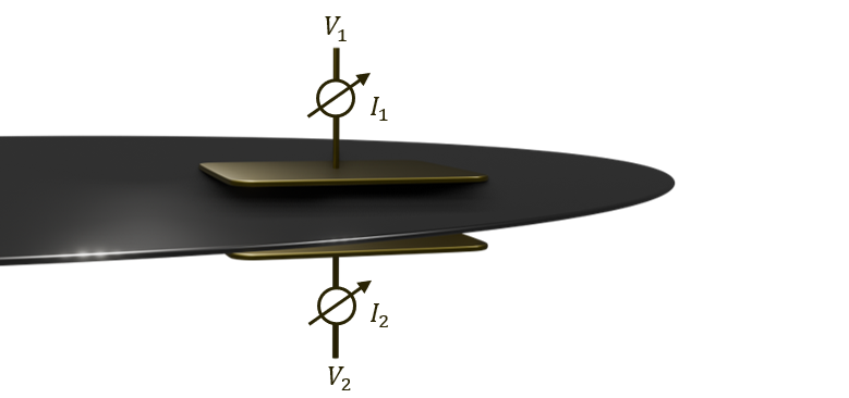
For conductive wafers, another effective non-contact method of measuring thickness is capacitive sensing. Capacitive measurement relies on changes in capacitance that occur when a conductive wafer is placed between two electrodes.
The capacitance depends on the distance (i.e., thickness) between the wafer surfaces and the electrodes, as well as the dielectric properties of the surrounding medium. By precisely measuring these changes in capacitance, the thickness of the wafer can be determined with high accuracy.
This method offers unique advantages for measuring conductive wafers, such as rapid response times, non-invasive measurements, and high precision. Capacitive measurement is particularly effective in applications where the wafer’s conductive properties play a critical role in determining overall performance.
We are here to help!
Information you provide in the form is used and stored to process your enquiry and, if you have allowed the cookies, to improve content personalisation.
SWS-Tec processes personal information responsibly. For more information, please review our Privacy Policy (General Data Protection Regulation/GDPR).
* Mandatory field
Office
D-85643 Steinhoering, Germany
Hours
M-F: 9am – 5pm
S-S: Closed
