MRes 2000M [200 mm] Software
Take Control with Our Advanced Device Control and Data Acquisition Software
MRes DataViz software
- 2d and 3d data analyzation
- 3d data point interpolation
- Direct comparison of different physical properties of the same wafer, for example Resistivity and Thickness
- Cross sectional analysis at arbitrary angles
- Data access via SQL Database
- One click export of a “Result Report pdf”, static and interactive figuree
- Individual Color Theme to reduce eye strain, optimal visibility and personal preference
Introducing Our MRes Data Analysis and Visualization Software
Unlock the full potential of your high precision data with our innovative software tailored for the semiconductor industry. Beyond just measuring, our software empowers you to delve deep into your data, providing insights that drive breakthroughs in research and development.
Here’s what sets our software apart:
- 2D and 3D Data Analysis: Gain comprehensive insights into your data with advanced analysis capabilities that extend into both two and three dimensions.
- 3D Data Point Interpolation: Seamlessly fill in the gaps in your data with precision through our sophisticated interpolation algorithms, ensuring a complete and accurate picture.
- Direct Comparison of Different Physical Properties: Easily compare various physical properties of the same wafer, such as resistivity and thickness, enabling you to identify correlations and optimize performance.
- Simultaneous Comparison of Same Physical Properties Across up to Four Wafers: Effortlessly compare the same physical property, such as resistivity, across up to four different wafers simultaneously. Gain deeper insights into material consistency and performance variation with ease.
- Cross Sectional Analysis at Arbitrary Angles: Explore your specimens from any angle with our flexible cross sectional analysis tools, providing a deeper understanding of their internal structures.
- Data Access via SQL Database: Effortlessly manage and retrieve your data with the power of SQL database integration, ensuring efficient workflows and seamless access to information.
- One Click Export of Result Reports: Streamline your reporting process with our intuitive one click export feature, giving you the opportunity of generating both PDF reports and static or dynamic figures with ease.
- Individual Color Themes: Customize your visualization experience with personalized color themes, reducing eye strain and enhancing visibility to suit your preferences.
At the forefront of innovation, our software is designed to empower semiconductor researchers and developers like you to unlock new insights, accelerate discoveries, and drive progress in the industry.
Take Control
with Our Advanced Device Control and Data Acquisition Software
Empower yourself with precision and efficiency in semiconductor research and development using our state-of-the-art device control and data acquisition software. Designed to streamline your workflow and maximize your productivity, our software offers unparalleled features tailored to meet your unique needs:
Customizable 2D Mapping Plans
Craft individual 2D mapping plans tailored to your specific requirements, allowing you to scan across semiconductor wafers with precision and flexibility.
Recipe Definition for Seamless Workflow
Define recipes encompassing crucial sample information and 2D mapping plans effortlessly. Capture vital details such as wafer material (e.g. Silicon or GaAs) and the presence of thin conductive layers, ensuring accurate data acquisition for diverse applications.
Live Data Acquisition with Comprehensive Visualization
Experience real-time data acquisition with insightful visualization tools. Our software provides live data displays, including 2D maps, histograms, and statistical analysis, empowering you to monitor and analyze your data with unparalleled clarity.
Seamless Data Management with SQL Database Integration
Effortlessly manage your data with seamless integration with SQL databases. Store your valuable data securely and access it with ease, ensuring efficient data retrieval and analysis whenever you need it.
Flexible Export Options for Enhanced Accessibility
Choose from automatic or manual export options for your data reports. Generate ASCII result reports containing comprehensive data sets effortlessly. Plus, with just one click, download 2D plots of your data and automatically generated result reports in PDF format for instant accessibility.
Customizable Display of Physical Properties
Tailor your data visualization to your specific needs by choosing which physical properties to display. Whether you’re measuring semiconductor wafer properties or thin conductive films, our software puts you in control.
Individual Color Themes
Customize your visualization experience with personalized color themes, reducing eye strain and enhancing visibility to suit your preferences.
Customize your visualization experience with personalized color themes, reducing eye strain and enhancing visibility to suit your preferences.
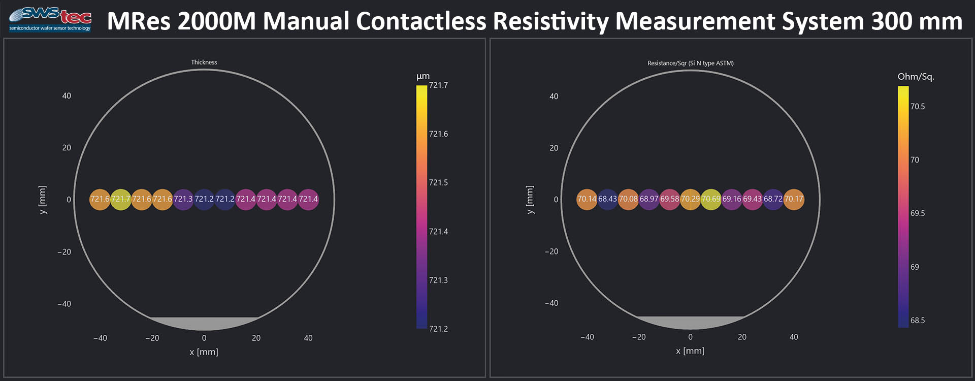
MRes2000M Manually Measured Mapping Result: The MRes2000M system provides manually measured mapping results, exemplified here for a Ø 100 mm Silicon wafer. Eleven distinct measurement points across the wafer are selected for measuring both thickness and resistance, allowing for the quantification of wafer quality.
3D Mapping – Sample thickness [µm]
The MRes 2000 Control Software showcases measurement results from a 49-point mapping plan, demonstrated here for a 100 mm Silicon wafer. The results are displayed in a color coded data plot, a histogram for easy visualization of data value distributi on, and a statistics table. Within the software, users can seamlessly switch between different physical quantities such as thickness, resistance, and resistivity.
Additionally, they have the option to toggle between raw and corrected values, adhering to the standards set by the American Society for Testing and Materials (ASTM).
Data Table – Resistance/Sqr (Si N type ASTM)
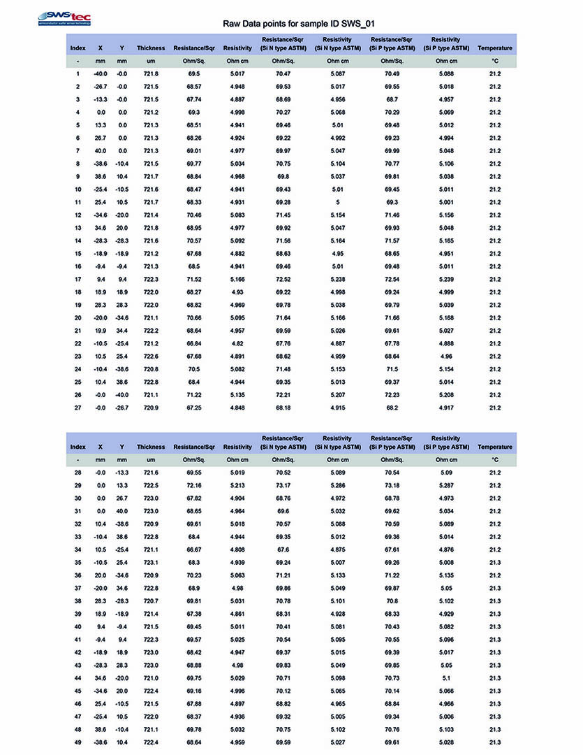
MRes 2000 Control Software presenting the measurement results of a 49 point mapping plan, exemplified here for a 100 mm Silicon wafer. Additionally to the graphical data representation all physical quantities can also be shown within a data-table.
Mapping – Resistance/Sqr (Si N type ASTM)
The MRes 2000 Control Software displays measurement results obtained from a custom made mapping plan, shaped like an Ohm symbol. Custom recipes, including mapping plans, are stored within a database, enabling users to easily select the required mapping plan for their current needs. Furthermore, the user can choose between different themes, including bright and dark representation of the control software.
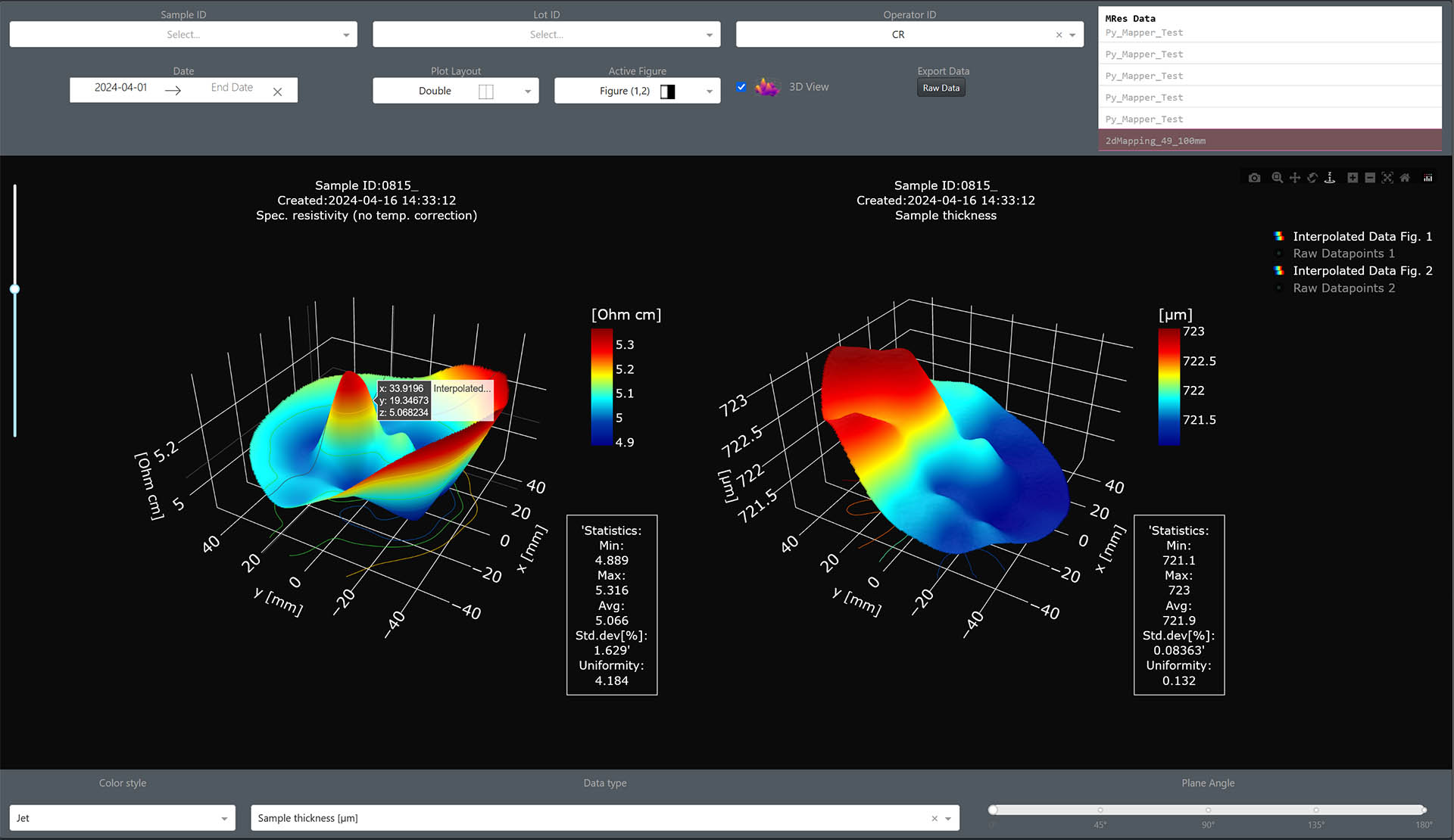
3D Mapping – Sample thickness [µm]
MRes Data Analysis and Visualization Software presenting a direct comparison between different physical quantities for the same specimen, as exemplified here for a Ø 100 mm Silicon wafer. The 3-dimensional views across multiple graphs can be synchronized, allowing for comfortable analysis of dependencies between different physical quantities, such as resistivity and thickness. We utilized 49 distinct measurement points across the wafer for thickness and resistance, enabling the calculation of 3-dimensional interpolated data.
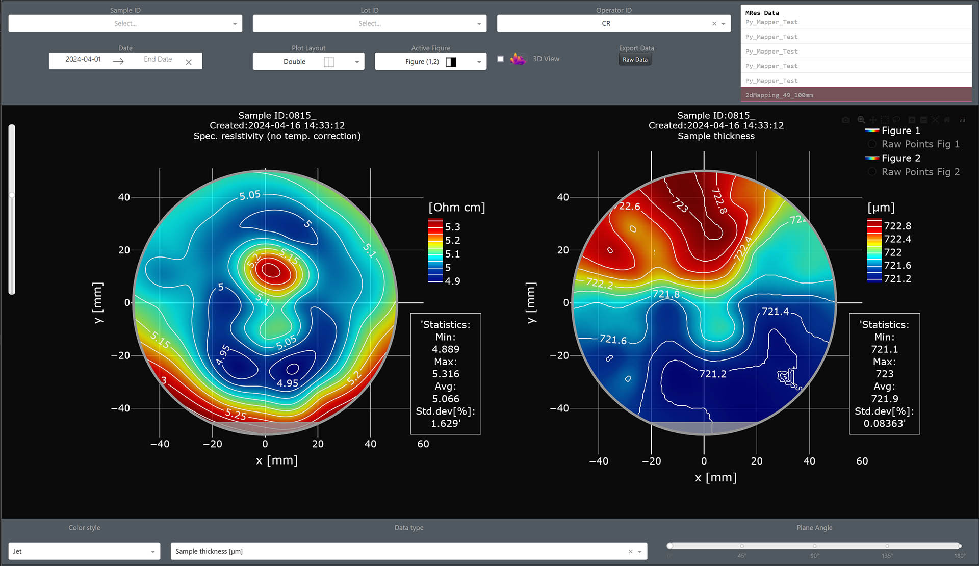
2D Mapping – Sample thickness [µm]
MRes Data Analysis and Visualization Software presenting a 2-dimensional view for the very same data presented in the left chart. We utilized 49 distinct measurement points across the wafer for thickness and resistance, enabling the calculation of the interpolated data.
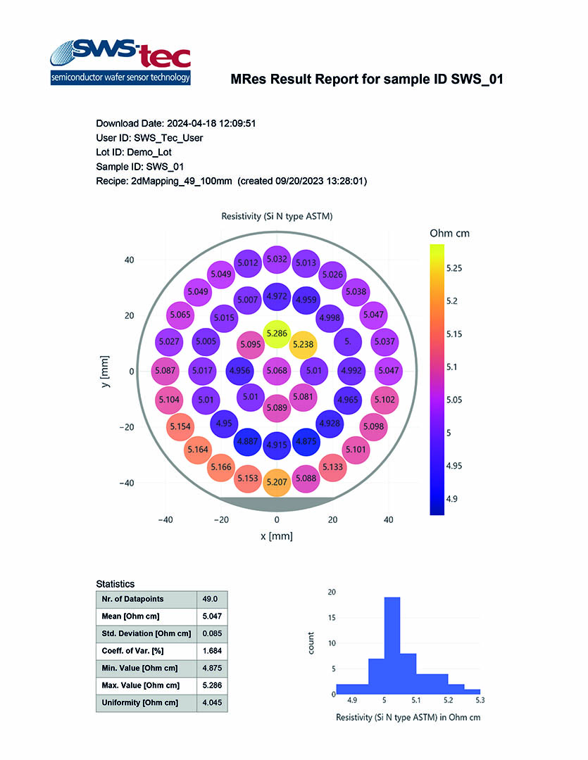
MRes Result Report.
MRes 2000 Control Software export functions: The export functions include automatically generated result reports in PDF format, ensuring comprehensive documentation of experimental outcomes, shown in (a). Additionally, the software facilitates exporting da ta in ASCII format, which offers flexibility for further analysis. Excel format is also supported, enabling seamless integration with existing data management systems.
Quick overview of experimental results.
Users can also download static images of color coded data plots, providing a quick overview of experimental results.
One click image download from our MRes Data Analysis and Visualization Software for a 3-dimensional cross section analysis and the corresponding 2-dimensional mapping points, shown in the top and bottom figure, respectively.
All physical quantities such as Thickness and Resistivity can be analyzed with the assistance of an interpolated cross-section area, indicated by the grey shaded plane in Fig. A. The cross-sectional data is presented in a separate graph (Fig. B) whereas the cross section can be rotated by 360°.
Utilizing 49 distinct measurement points distributed across the wafer, as shown in Fig. C allows for precise calculation of the interpolated data. The data showcased in this figure was acquired from a Ø 300 mm Silicon wafer.
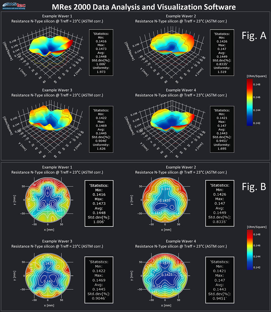
Comparison between up to four different datasets within our MRes Data-Analysis and Visualization Software in both, 3-dimensional (Fig. A) or 2-dimensional (Fig. B) presentation. Simply choose between the same physical quantity for different wafers (presented in this figure ), different physical quantities for the same wafer (not shown within this figure) or a mixture of both.
We utilized 49 distinct measurement points across the wafer for Thickness and Resistance, enabling the calculation of 3-dimensional interpolated data. The data showcased in these figures was acquired from four different Silicon wafers.
MRes 2000 Contactless Resistivity Measurement System
Wafer size | up to 300 mm |
Wafer thickness: | 150 µm up to 1,200 µm |
Resistance range: | < 0.01 Ohm/sq |
> 15 kOhm/sq |
|
Std.dev[%]: | 0.01 @ 0.06 Ohm/sq |
(10 data pts.) | 0.04 @ 34 Ohm/sq |
0.33 @ 5,000 Ohm/sq |
We're Here To Help!
Office
D-85598 Baldham, Germany
Hours
M-F: 8am – 5pm
S-S: Closed
Call Us
+49-8106 3 94 81 46
